2020 官网升级中!现在您访问官网的浏览器设备分辨率宽度低于1280px请使用高分辨率宽度访问。

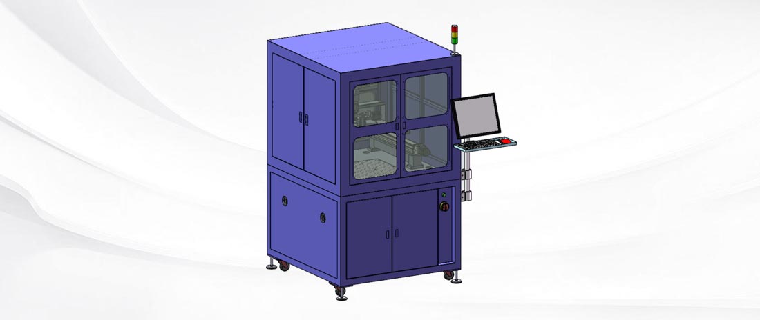
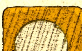
Wafer AVI is used to detect various defects of semiconductor wafers in the process of manufacturing. Through multi-station optical imaging settings, the corresponding size and defect problems are respectively detected to ensure full coverage of defects. Combined with a variety of detection algorithms, it ensures good detection results and achieves better stable applications.
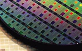
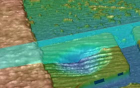
Foreign bodies, hanging burrs, breakage, filaments, contaminated particles, warping, and corresponding dimensional measurements

 Wechat
 Online Service


Learn more about AVI
To become the world's most innovative machine vision products and solutions provider
 WeChat Account